[ comments ]
“Secure Element” (SE) chips have traditionally taken a very closed-source, NDA-heavy approach. Thus, it piqued my interest when an early-stage SE chip startup, Cramium (still in stealth mode), approached me to advise on open source strategy. This blog post explains my reasoning for agreeing to advise Cramium, and what I hope to accomplish in the future.
As an open source hardware activist, I have been very pleased at the progress made by the eFabless/Google partnership at creating an open-to-the-transistors physical design kit (PDK) for chips. This would be about as open as you can get from the design standpoint. However, the partnership currently supports only lower-complexity designs in the 90nm to 180nm technology nodes. Meanwhile, Cramium is planning to tape out their security chip in the 22nm node. A 22nm chip would be much more capable and cost-effective than one fabricated in 90nm (for reference, the RP2040 is fabricated in 40nm, while the Raspberry Pi 4’s CPU is fabricated in 28nm), but it would not be open-to-the-transistors.
Cramium indicated that they want to push the boundaries on what one can do with open source, within the four corners of the foundry NDAs. Ideally, a security chip would be fabricated in an open-PDK process, but I still feel it’s important to engage and help nudge them in the right direction because there is a genuine possibility that an open SDK (but still closed PDK) SE in a 22nm process could gain a lot of traction. If it’s not done right, it could establish poor de-facto standards, with lasting impacts on the open source ecosystem.
For example, when Cramium approached me, their original thought was to ship the chip with an ARM Cortex M7 CPU. Their reasoning is that developers prize a high-performance CPU, and the M7 is one of the best offerings in its class from that perspective. Who doesn’t love a processor with lots of MHz and a high IPC?
However, if Cramium’s chip were to gain traction and ship to millions of customers, it could effectively entrench the ARM instruction set — and more importantly — quirks such as the Memory Protection Unit (MPU) as the standard for open source SEs. We’ve seen the power of architectural lock-in as the x86 serially shredded the Alpha, Sparc, Itanium and MIPS architectures; so, I worry that every new market embracing ARM as a de-facto standard is also ground lost to fully open architectures such as RISC-V.
So, after some conversations, I accepted an advisory position at Cramium as the Ecosystem Engineer under the condition that they also include a RISC-V core on the chip. This is in addition to the Cortex M7. The good news is that a RISC-V core is royalty-free, and the silicon area necessary to add it at 22nm is basically a rounding error in cost, so it was a relatively easy sell. If I’m successful at integrating the RISC-V core, it will give software developers a choice between ARM and RISC-V.
So why is Cramium leaving the M7 core in? Quite frankly, it’s for risk mitigation. The project will cost upwards of $20 million to tape out. The ARM M7 core has been taped out and shipped in millions of products, and is supported by a billion-dollar company with deep silicon experience. The VexRiscv core that we’re planning to integrate, on the other hand, comes with no warranty of fitness, and it is not as performant as the Cortex M7. It’s just my word and sweat of brow that will ensure it hopefully works well enough to be usable. Thus, I find it understandable that the people writing the checks want a “plan B” that involves a battle-tested core, even if proprietary.
This will understandably ruffle the feathers of the open source purists who will only certify hardware as “Free” if and only if it contains solely libre components. I also sympathize with their position; however, our choices are either the open source community somehow provides a CPU core with a warranty of fitness, effectively underwriting a $20 million bill if there is a fatal bug in the core, or I walk away from the project for “not being libre enough”, and allow ARM to take the possibly soon-to-be-huge open source SE market without challenge.
In my view it’s better to compromise and have a seat at the table now, than to walk away from negotiations and simply cede green fields to proprietary technologies, hoping to retake lost ground only after the community has achieved consensus around a robust full-stack open source SE solution. So, instead of investing time arguing over politics before any work is done, I’m choosing to invest time building validation test suites. Once I have a solid suite of tests in hand, I’ll have a much stronger position to argue for the removal of any proprietary CPU cores.
On the Limit of Openness in a Proprietary Ecosystem
Advising on the CPU core is just one of many tasks ahead of me as their open source Ecosystem Engineer. Cramium’s background comes from the traditional chip world, where NDAs are the norm and open source is an exotic and potentially fatal novelty. Fatal, because most startups in this space exit through acquisition, and it’s much harder to negotiate a high acquisition price if prized IP is already available free-of-charge. Thus my goal is to not alienate their team with contumelious condescension about the obviousness and goodness of open source that is regrettably the cultural norm of our community. Instead, I am building bridges and reaching across the aisle, trying to understand their concerns, and explaining to them how and why open source can practically benefit a security chip.
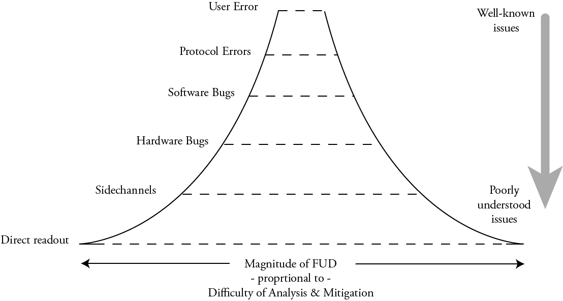
To that end, trying to figure out where to draw the line for openness is a challenge. The crux of the situation is that the perceived fear/uncertainty/doubt (FUD) around a particular attack surface tends to have an inverse relation to the actual size of the attack surface. This illustrates the perceived FUD around a given layer of the security hierarchy:
Generally, the amount of FUD around an attack surface grows with how poorly understood the attack surface is: naturally we fear things we don’t understand well; likewise we have less fear of the familiar. Thus, “user error” doesn’t sound particularly scary, but “direct readout” with a focused ion beam of hardware security keys sounds downright leet and scary, the stuff of state actors and APTs, and also of factoids spouted over beers with peers to sound smart.
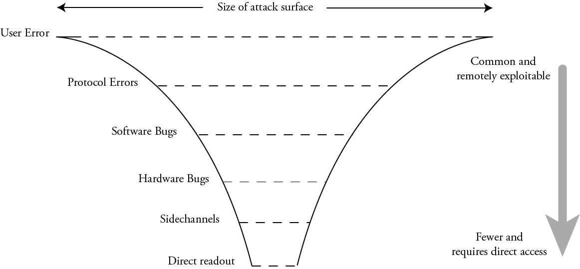
However, the actual size of the attack surface is quite the opposite:
In practice, “user error” – weak passwords, spearphishing, typosquatting, or straight-up fat fingering a poorly designed UX – is common and often remotely exploitable. Protocol errors – downgrade attacks, failures to check signatures, TOCTOUs – are likewise fairly common and remotely exploitable. Next in the order are just straight-up software bugs – buffer overruns, use after frees, and other logic bugs. Due to the sheer volume of code (and more significantly the rate of code turnover) involved in most security protocols, there are a lot of bugs, and a constant stream of newly minted bugs with each update.
Beneath this are the hardware bugs. These are logical errors in the implementation of a function of a piece of hardware, such as memory aliasing, open test access ports, and oversights such as partially mutable cryptographic material (such as an AES key that can’t be read out, but can be updated one byte at a time). Underneath logical hardware bugs are sidechannels – leakage of secret information through timing, power, and electromagnetic emissions that can occur even if the hardware is logically perfect. And finally, at the bottom layer is direct readout – someone with physical access to a chip directly inspecting its arrangement of atoms to read out secrets. While there is ultimately no defense against the direct readout of nonvolatile secrets short of zeroizing them on tamper detection, it’s an attack surface that is literally measured in microns and it requires unmitigated physical access to hardware – a far cry from the ubiquity of “user error” or even “software bugs”.
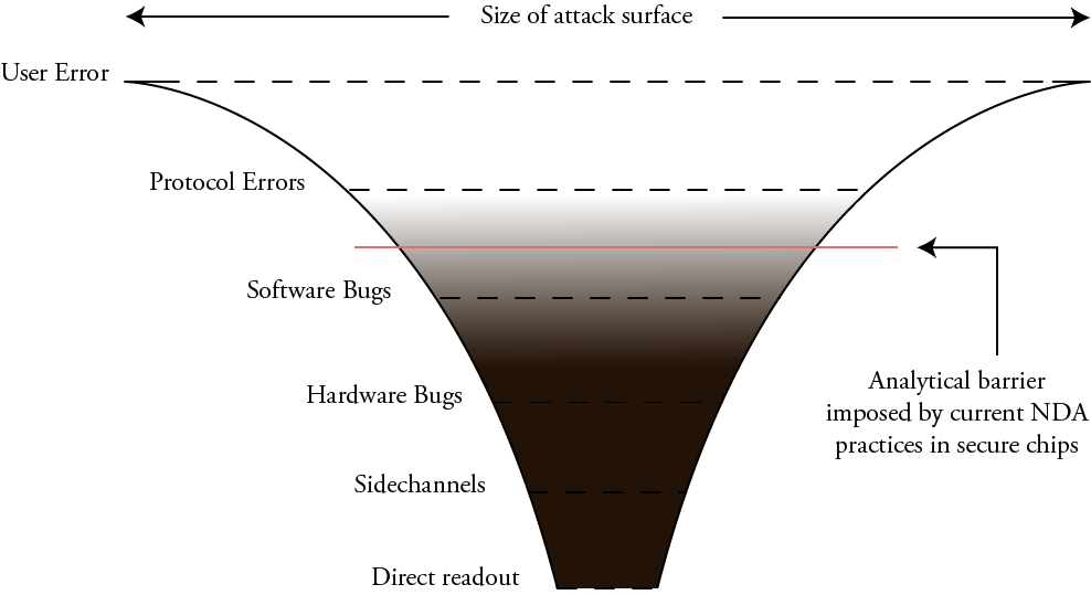
The current NDA-heavy status quo for SE chips creates an analytical barrier that prevents everyday users like us from determining how big the actual attack surface is. That analytical barrier actually extends slightly up the stack from hardware, into “software bugs”. This is because without intimate knowledge of how the hardware is supposed to function, there are important classes of software bugs we can’t analyze.
Furthermore, the inability of developers to freely write code and run it directly on SEs forces more functionality up into the protocol layer, creating an even larger attack surface.
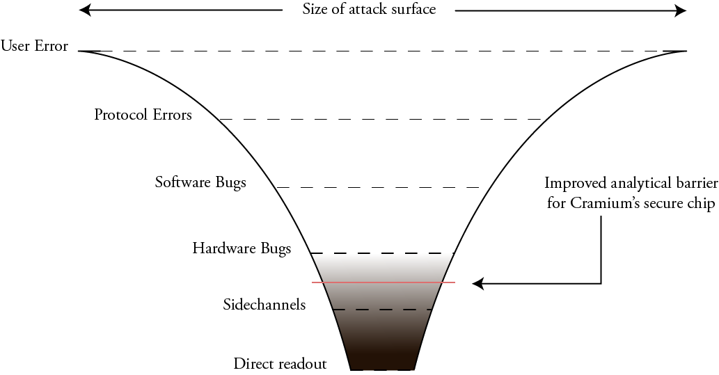
My hope is that working with Cramium will improve this situation. In the end, we won’t be able to entirely remove all analytical barriers, but hopefully we arrive at something closer to this:
Due to various NDAs, we won’t be able to release things such as the mask geometries, and there are some blocks less relevant to security such as the ADC and USB PHY that are proprietary. However, the goal is to have the critical sections responsible for the security logic, such as the cryptographic accelerators, the RISC-V CPU core, and other related blocks shared as open source RTL descriptions. This will allow us to have improved, although not perfect, visibility into a significant class of hardware bugs.
The biggest red flag in the overall scenario is that the on-chip interconnect matrix is slated to be a core generated using the ARM NIC-400 IP generator, so this logic will not be available for inspection. The reasoning behind this is, once again, risk mitigation of the tapeout. This is unfortunate, but this also means we just need to be a bit more clever about how we structure the open source blocks so that we have a toolbox to guard against potential misbehavior in the interconnect matrix.
My personal goal is to create a fully OSS-friendly FPGA model of the RISC-V core and their cryptographic accelerators using the LiteX framework, so that researchers and analysts can use this to model the behavior of the SE and create a battery of tests and fuzzers to confirm the correctness of construction of the rest of the chip.
In addition to the work advising Cramium’s engagement with the open source community, I’m also starting to look into non-destructive optical inspection techniques to verify chips in earnest, thanks to a grant I received from NLNet’s NGI0 Entrust fund. More on this later, but it’s my hope that I can find a synergy between the work I’m doing at Cramium and my silicon verification work to help narrow the remaining gaps in the trust model, despite refractory foundry and IP NDAs.
Counterpoint: The Utility of Secrecy in Security
Secrecy has utility in security. After all, every SE vendor runs with this approach, and for example, we trust the security of nuclear stockpiles to hardware that is presumably entirely closed source.
Secrecy makes a lot of sense when:
- Even a small delay in discovering a secret can be a matter of life or death
- Distribution and access to hardware is already strictly controlled
- The secrets would rather be deleted than discovered
Military applications check all these boxes. The additional days, weeks or months delay incurred by an adversary analyzing around some obfuscation can be a critical tactical advantage in a hot war. Furthermore, military hardware has controlled distribution; every mission-critical box can be serialized and tracked. Although systems are designed assuming serial number 1 is delivered to the Kremlin, great efforts are still taken to ensure that is not the case (or that a decoy unit is delivered), since even a small delay or confusion can yield a tactical advantage. And finally, in many cases for military hardware, one would rather have the device self-destruct and wipe all of its secrets, rather than have its secrets extracted. Building in booby traps that wipe secrets can measurably raise the bar for any adversary contemplating a direct-readout attack.
On the other hand, SEs like those found in bank cards and phones are:
- Widely distributed – often directly and intentionally to potentially adversarial parties
- Protecting data at rest (value of secret is constant or may even grow with time)
- Used as a trust root for complicated protocols that typically update over time
- Protecting secrets where extraction is preferable to self-destruction. The legal system offers remedies for recourse and recovery of stolen assets; whereas self-destruction of the assets offers no recourse
In this case, the role of the anti-tamper countermeasures and side-channel minimization is to raise the investment necessary to recover data from “trivial” to somewhere around “there’s probably an easier and cheaper way to go about this…right?”. After all, for most complicated cryptosystems, the bigger risk is an algorithmic or protocol flaw that can be exploited without any circumvention of hardware countermeasures. If there is a protocol flaw, employing an SE to protect your data is like using a vault, but leaving the keys dangling on a hook next to the vault.
It is useful to contemplate who bears the greatest risk in the traditional SE model, where chips are typically distributed without any way to update their firmware. While an individual user may lose the contents of their bank account, a chip maker may bear a risk of many tens of millions of dollars in losses from recalls, replacement costs and legal damages if a flaw were traced to their design issue. In this game, the player with the most to lose is the chipmaker, not any individual user protected by the chip. Thus, a chipmaker has little incentive to disclose their design’s details.
A key difference between a traditional SE and Cramium’s is that Cramium’s firmware can be updated (assuming an updateable SKU is released; this was a surprisingly controversial suggestion when I brought it up). This is thanks in part to the extensive use of non-volatile ReRAM to store the firmware. This likewise shifts the calculus on what constitutes a recall event. The open source firmware model also means that the code on the device comes, per letter of the license, without warranty; the end customer is ultimately responsible for building, certifying and deploying their own applications. Thus, for a player like Cramium, the potential benefits of openness outweigh those of secrecy and obfuscation embraced by traditional SE vendors.
Summary
My role is to advise Cramium on how to shift the norms around SEs from NDAs to openness. Cramium is not attempting to forge an open-foundry model – they are producing parts using a relatively advanced (compared to your typical stand-alone SE) 22nm process. This process is protected by the highly restrictive foundry NDAs. However, Cramium plans to release much of their design under an open source license, to achieve the following goals:
- Facilitate white-box inspection of cryptosystems implemented using their primitives
- Speed up discovery of errors; and perhaps more importantly, improve the rate at which they are patched
- Reduce the risk of protocol and algorithmic errors, so that hardware countermeasures could be the actual true path of least resistance
- Build trust
- Promote wide adoption and accelerate application development
Cramium is neither fully open hardware, nor is it fully closed. My goal is to steer it toward the more open side of the spectrum, but the reality is there are going to be elements that are too difficult to open source in the first generation of the chip.
The Cramium chip complements the eFabless/Google efforts to build open-to-the-transistors chips. Today, one can build chips that are open to the mask level using 90 – 180nm processes. Unfortunately, the level of integration achievable with their current technology isn’t quite sufficient for a single-chip Secure Element. There isn’t enough ROM or RAM available to hold the entire application stack on chip, thus requiring a multi-chip solution and negating the HSM-like benefits of custom silicon. The performance of older processes is also not sufficient for the latest cryptographic systems, such as Post Quantum algorithms or Multiparty Threshold ECDSA with Identifiable Aborts. On the upside, one could understand the design down to the transistor level using this process.
However, it’s important to remember that knowing the mask pattern does not mean you’ve solved the supply chain problem, and can trust the silicon in your hands. There are a lot of steps that silicon goes through to go from foundry to product, and at any of those steps the chip you thought you’re getting could be swapped out with a different one; this is particularly easy given the fact that all of the chips available through eFabless/Google’s process use a standardized package and pinout.
In the context of Cramium, I’m primarily concerned about the correctness of the RTL used to generate the chip, and the software that runs on it. Thus, my focus in guiding Cramium is to open sufficient portions of the design such that anyone can analyze the RTL for errors and weaknesses, and less on mitigating supply-chain level attacks.
That being said, RTL-level transparency can still benefit efforts to close the supply chain gap. A trivial example would be using the RTL to fuzz blocks with garbage in simulation; any differences in measured hardware behavior versus simulated behavior could point to extra or hidden logic pathways added to the design. Extra backdoor circuitry injected into the chip would also add loading to internal nodes, impacting timing closure. Thus, we could also do non-destructive, in-situ experiments such as overclocking functional blocks to the point where they fail; with the help of the RTL we can determine the expected critical path and compare it against the observed failure modes. Strong outliers could indicate tampering with the design. While analysis like this cannot guarantee the absence of foundry-injected backdoors, it constrains the things one could do without being detected. Thus, the availability of design source opens up new avenues for verifying correctness and trustability in a way that would be much more difficult, if not impossible, to do without design source.
Finally, by opening as much of the chip as possible to programmers and developers, I’m hoping that we can get the open source SE chip ecosystem off on the right foot. This way, as more advance nodes shift toward open PDKs, we’ll be ready and waiting to create a full-stack open source solution that adequately addresses all the security needs of our modern technology ecosystem.
[ comments ]


